Forget GPUs, A Memory Chip Squeeze Could Choke AI Even After OpenAI’s $250B Splurge
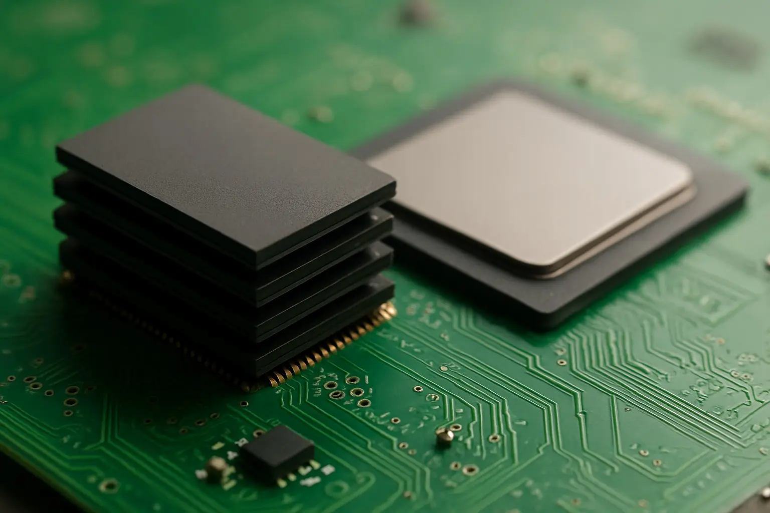
OpenAI has signed up for $250 billion more of Microsoft‘s cloud, but AI’s next limit may be the memory chips packed beside every AI processor, made by a few suppliers and hard to scale fast.
TL;DR
- The next bottleneck in AI is not just compute wafers. It is the full assembly path from logic die to HBM4 stacks to advanced packaging, where capacity is concentrated and hard to expand quickly.
- HBM4 changes the system design equation by raising bandwidth and density options, but it also deepens dependence on packaging precision, buffer dies, thermals and memory supply coordination.
- Control of next-generation inference scale will come from whoever can secure integrated supply, not whoever simply announces the largest model.
For most of the past three years, AI competition was described as a software race dressed in semiconductor clothing.
Now JEDEC published the HBM4 and SPHBM4 standards in 2026, TSMC scheduled A14 risk production for the first quarter of 2026, and filings show OpenAI contracted an incremental $250 billion of Azure services, all of which makes the fight over the HBM4 supply chain, package substrates and assembly capacity more important than raw model design.
Why The Bottleneck Moved From Wafers To Packages
The popular picture of AI hardware scarcity still starts and ends with leading-edge process nodes. That was useful when the key question was whether enough 5 nm and 4 nm GPU die could be fabricated. It is less useful now.
Modern AI accelerators are systems in package, with multiple logic tiles, multiple HBM stacks, an interposer or bridge layer, high-density substrate work, and increasingly a thermal design problem that determines whether the theoretical memory bandwidth can be used in production. The HBM4 supply chain ties those elements together, if HBM4 stacks, buffer dies or interposers are delayed, a completed logic die cannot be deployed at scale.
Foundries can print a leading die, but module-level production depends on third-party assembly partners, interposer availability, substrate supply and mature underfill and test flows. TSMC’s CoWoS positioning and Intel’s Foveros Direct 3D briefings are examples firms use to show they can coordinate those parts of the HBM4 supply chain. Publicly available materials from both companies emphasize packaging platforms as strategic offerings rather than incidental services.
This dynamic is why Intel’s AIB and Foveros messaging matters to the HBM4 supply chain debate. Intel wrote that AIB moves data via microbumps between adjacent devices and relies on fine-pitch high-density packaging. That technical detail has market consequences because it ties a design’s performance to specific packaging capabilities and qualified assembly partners.
JEDEC’s SPHBM4 and HBM4 standards are direct evidence of diverging hardware strategies within the HBM4 supply chain. SPHBM4 targets reduced pin counts with serialization while HBM4 maximizes direct-attached bandwidth, and both standards materially change substrate routing and interposer requirements for production-ready modules.
The Chiplet Era Made Packaging The Product
Chiplets are often pitched as a route to modularity, faster reuse and better yields. All of that is true. But for AI accelerators, the deeper effect is that packaging stops being back-end plumbing and becomes part of the core architecture.
A multi-die accelerator only works if the package can preserve bandwidth and power characteristics close enough to what a monolithic design would have offered. That is why Intel said Foveros Direct 3D is aimed at AI and HPC integration, and why the company keeps framing advanced chiplet packaging as a foundry service rather than a supporting capability. The package is doing architectural work.
Intel also said its Foveros technology has been in mass production since 2019 with an active base die. That matters less as a brag than as a signal that packaging credibility now requires proof of manufacturability over multiple generations. Everyone in this market can show a roadmap slide. Far fewer can show years of high-complexity production.
TSMC has the same advantage from a different direction. Its CoWoS platform is now not just one packaging option among many but the reference point around which much of AI accelerator supply planning is organized. When customers reserve leading AI capacity, they are effectively reserving a combined stack of wafer starts, HBM attachment, interposer work, advanced test and package output.
Each layer has different lead times, equipment dependencies and yield curves. That is the core HBM4 supply chain change, the unit of scarcity is no longer the die but the finished accelerator module.
Standardized die-to-die connectivity could, over time, lower switching costs between design blocks or packaging strategies. JEDEC’s SPHBM4 work shows one practical route to lower pin-count designs, but in the nearer term the more sophisticated the package, the more tightly integrated supplier relationships become. Standardization may help design portability. It does not magically create more high-yield package output.
HBM4 Supply Chain Rewrites The Memory Side Of The Equation
The HBM4 transition is not just a routine memory upgrade. It changes package design, interconnect count, stack options and potentially the kinds of accelerators that can reach acceptable bandwidth per watt in large-scale inference.
JEDEC published that HBM4 supports 4-high, 8-high, 12-high and 16-high stack configurations using 24 Gb or 32 Gb die densities. At the high end, that creates a much wider design space for accelerator vendors. They can push more capacity into a package, chase higher bandwidth, or balance the two depending on workload mix and thermal headroom.
The interface itself is also bigger. JEDEC said HBM4 uses 2,048 data signals, while SPHBM4 defines 512 data signals with 4:1 serialization to target the same throughput with reduced pin count. That is not a minor standards footnote. It points to two diverging paths for AI hardware within the HBM4 supply chain.
JEDEC’s main-memory taxonomy disclosed that SPHBM4 was published in June 2026. The timing matters. It arrived just as AI buyers were discovering that memory bandwidth is not an abstract specification but a commercial chokepoint. Larger reasoning models, retrieval-heavy agent workloads and longer-lived conversational sessions all push memory systems differently from the image and training-dominant workloads of the earlier GPU boom.
HBM4 also tightens coupling between memory and package roadmaps. Higher bandwidth is only valuable if the package can route, power and cool the stack without collapsing yields. In that sense, HBM4 strengthens the grip of suppliers that can coordinate the whole module. A weak point anywhere in the HBM4 supply chain, buffer die readiness, interposer availability, underfill process maturity or substrate supply, turns into a product delay.
The near-term sign of where the industry expects value to accrue is the IP layer around HBM4E and leading nodes. GUC announced 2 nm 16 Gbps HBM4E IP in Sept. 2026. Even without broad public pricing or volume commitments, that announcement shows where design ecosystems are spending ahead of demand, memory interfaces, not just compute cores.
That investment is a concrete indicator of where the HBM4 supply chain bottlenecks will matter most.
TSMC Controls The Narrowest Part Of The Pipe
If the HBM4 supply chain has a single central node, it is TSMC. Not because every future AI accelerator will be built there, but because the company sits closest to the combination of leading logic, packaging scale and ecosystem gravity that customers actually need in the same program.
TSMC announced that A14 is scheduled to enter risk production in the first quarter of 2026. Risk production is not volume output, and it does not guarantee rapid AI deployment. But it does reveal how early large customers can begin preparing designs intended to converge with later packaging and memory transitions.
For a company trying to ship next-generation inference silicon in volume around the end of the decade, node and packaging roadmaps must be synchronized years earlier. The ecosystem layer matters too. TSMC’s OIP forum materials showed how broadly the company organizes design partners, IP, EDA and packaging-adjacent suppliers around its process roadmap.
In practice, that makes TSMC more than a fab. It is the coordination point where chiplet plans, HBM interfaces, test flows and customer schedules become mutually dependent. This concentration is most visible in CoWoS.
The company’s packaging page does not disclose a neat public capacity line, but its prominence in the 3DFabric stack makes clear that advanced packaging is being productized as a strategic platform, not sold as a commodity service. The market consequence is that customers do not merely shop for manufacturing. They queue for a workflow.
That queue affects bargaining power in ways visible in public filings and partnerships. Large customers have signed multi-year reservations and contracts that effectively prioritize their access to limited module-level capacity, OpenAI’s incremental $250 billion Azure commitment, AMD’s strategic partnership to become a core compute partner for OpenAI, and reported expansions in Broadcom, Google and Anthropic compute relationships all show how demand is being reserved in advance.
When suppliers’ order books are dense, that reservation discipline can tilt capacity toward hyperscalers and away from smaller cloud providers or second-tier accelerator startups, and switching providers mid-cycle can become difficult even if a rival foundry advertises similar node performance.
This is why next-generation inference scale looks less like a pure performance contest and more like a logistics contest. The chip that matters is the one that arrives in volume, with memory attached, inside a power envelope customers can deploy. The HBM4 supply chain is the mechanism that turns wafer output into deployable inference capacity.
| Supply-chain lever | Public figure | Why it matters | Source |
|---|---|---|---|
| A14 timeline | Risk production in Q1 2026 | Sets earliest window for future leading-edge AI designs | TSMC press release |
| HBM4 interface | 2,048 data signals | Increases package routing and integration complexity | JEDEC SPHBM4 release |
| SPHBM4 interface | 512 data signals with 4:1 serialization | Potential alternative path to HBM4-class throughput with lower pin count | JEDEC SPHBM4 release |
| HBM4 stack options | 4-high, 8-high, 12-high, 16-high | Expands capacity and bandwidth design choices | JEDEC HBM4 release |
| HBM4 die density | 24 Gb or 32 Gb | Determines package capacity ceilings | JEDEC HBM4 release |
| H100 memory | 80 GB HBM | Baseline for current-generation accelerator memory scaling | Nvidia whitepaper/blog |
| OpenAI Azure commitment | Incremental $250B services purchase | Signals how much future accelerator capacity large customers may absorb | Microsoft exhibit |
Also Read: AMEC Eyes Korean Power Chip Wins As AI Server Racks Face Supply Risk In Trials
Nvidia Set The Template, But The Template Gets Harder To Copy
Nvidia’s success came partly from software and partly from shipping complete systems while competitors were still arguing over architecture. But the company’s recent hardware disclosures show why the rest of the industry is converging on the same bottlenecks within the HBM4 supply chain.
Nvidia showed a progression in GPU HBM capacity from the Hopper H100 at 80 GB through later generations, while its reasoning-era system material reported 20 TB of HBM memory and 40 TB of fast memory at the system level.
Even if those figures sit at different layers of the stack, they point in the same direction, AI vendors are no longer optimizing a chip in isolation. They are optimizing a memory-rich, networked, package-intensive machine.
The original Hopper documentation already hinted at this. Nvidia published that H100 used an HBM3 and HBM2e DRAM subsystem, underscoring that the memory architecture was central to performance, not decorative. The Blackwell and post-Blackwell roadmaps simply make that fact unavoidable.
For competitors, that creates a difficult copying problem. It is not enough to match arithmetic throughput. They need to match memory capacity, bandwidth, package assembly competence, software stack maturity and delivery reliability at once. The more memory-heavy inference becomes, the more difficult that package-level replication gets within the HBM4 supply chain.
One underappreciated consequence is that even large buyers may prefer ecosystem diversity not because they can easily replace Nvidia, but because dependence on a single packaged-systems pipeline introduces procurement risk. A second source with somewhat lower peak performance can still be strategically valuable if it guarantees capacity when the primary line is constrained.
Contracts, Not Benchmarks, Decide Who Gets Scale
The cleanest evidence that AI supply is shifting from open-market procurement to reserved industrial capacity appears in customer contracts and filings, not benchmark charts. A Microsoft exhibit disclosed that OpenAI contracted to purchase an incremental $250 billion of Azure services, while Microsoft remains OpenAI’s compute provider.
That figure is large, but its strategic value is even larger than its size, it implies future accelerator output is increasingly spoken for years in advance through cloud commitments rather than bought opportunistically once products ship.
Another filing reported that Broadcom, Google and Anthropic expanded their AI compute relationship, with Anthropic’s consumption dependent on deployment of that capacity. That caveat is important, demand alone does not create inference scale. Deployment-ready infrastructure does.
The same pattern is visible in supplier diversification. An AMD exhibit announced a strategic partnership making AMD a core compute partner for OpenAI, building on collaboration that began with MI300X. That does not mean AMD suddenly breaks the packaging bottleneck. It means top customers are paying to create optionality against it.
One less discussed consequence of these contracts is that they may reshape innovation at the model layer. If compute reservations are concentrated among a handful of hyperscalers and labs, then the practical frontier is set not only by algorithmic advances but by who has pre-bought enough HBM4 supply chain certainty to exploit them.
A better model without secured package output may lose to a slightly worse model with guaranteed deployment capacity. That is why the future AI market may stratify into three layers. First are the integrated hyperscaler-lab blocs that secure logic, memory, packaging and data center deployment as one plan.
Second are large enterprises and sovereign buyers that obtain scale through those blocs. Third are everyone else, who may access frontier models through APIs but not control the underlying hardware roadmap.
What Next-generation Inference Scale Actually Requires
The phrase “inference scale” gets used loosely, as if it simply means more GPUs in more data centers. The hardware evidence points to a more specific definition. Next-generation inference scale means sustaining high-volume, latency-sensitive, memory-intensive serving across increasingly interactive workloads. That requires at least five things.
First, enough logic die output at sufficiently advanced nodes. This is still necessary, just no longer sufficient.
Second, enough HBM4 or HBM4-adjacent memory supply. HBM4 expands design options, but every extra stack deepens dependence on memory vendors, buffer technology and package assembly quality. The HBM4 supply chain ties memory vendors, buffer-die makers and OSATs into a single delivery path.
Third, package technologies that can keep chiplets and memory fed without unacceptable thermal or yield penalties. Intel’s Foveros materials and TSMC’s CoWoS positioning both make clear that advanced packaging is where these tradeoffs now live.
Fourth, credible interconnect standards. Chiplet systems become less attractive if every vendor’s package is a locked island. Standard interfaces like JEDEC’s SPHBM4 could reduce switching costs and broaden supplier options inside the HBM4 supply chain.
Fifth, customer contracts that justify all of the above. Supply chains scale on demand visibility. The labs and clouds signing large commitments are not only buying compute. They are underwriting upstream capital expenditure in foundries, OSAT-like functions, testing and memory ecosystems.
There is also a power and utilization angle. Large reasoning and agent workloads tend to keep more state alive per session than earlier bursty chatbot interactions. That may increase the commercial value of memory capacity and memory locality relative to peak flop claims.
In other words, the winner in 2028 may not be the accelerator with the most impressive launch-day benchmark. It may be the one that delivers the best memory-backed token economics in steady-state production through a robust HBM4 supply chain.
Methodology
This piece examined primary documents published or updated through Tuesday, Oct. 20, 2026, including TSMC process and ecosystem materials, Intel packaging briefs and white papers, Nvidia architecture disclosures, JEDEC memory standards releases, and SEC-filed exhibits and 8-K materials tied to major AI compute relationships.
The analysis focused on the 2026 through 2030 supply chain for AI accelerators, with special attention to four linked constraints, chiplet interconnects, HBM4 and SPHBM4 standards, advanced packaging, and customer compute commitments. It prioritized disclosed figures over industry rumor.
Evidence is thin in several places. Public documents rarely disclose package yield, exact CoWoS or Foveros output, HBM4 pricing, wafer allocation by customer, or the detailed volume terms behind most private cloud reservations. It was also not possible to independently verify how quickly SPHBM4 will be adopted in commercial accelerators, or whether announced partnerships translate into material 2027 to 2028 shipments on the timelines implied by marketing.
The Counterargument
The strongest case against this thesis is that the industry may be overestimating how much future inference depends on the most advanced packaging path. JEDEC’s SPHBM4 track suggests one alternative. If reduced-pin-count implementations can deliver HBM4-class throughput in more conventional package forms, then the most acute pressure on ultra-complex package assembly could ease.
That would not eliminate memory scarcity, but it could widen the supplier base and lower the advantage of the incumbents with the hardest 2.5D or 3D packaging capability in the HBM4 supply chain.
There is also a software-and-systems argument. Better quantization, smarter caching, distillation, speculative decoding and workload-specific accelerators could reduce how much premium HBM is required per served token. If that happens fast enough, the market may discover that 2027 to 2030 inference growth is more tolerant of diverse hardware than the current procurement cycle implies.
A third objection is competitive. Intel has years of packaging investment behind Foveros, AMD is already inside top-lab compute planning, and custom silicon buyers continue to work with partners such as Broadcom. If enough viable second sources emerge, then TSMC’s control over the narrowest part of the pipe may weaken before the decade ends.
Those are serious objections. But they do not erase the present evidence. Right now, the disclosed standards, roadmaps and contracts all point in the same direction, AI scale is becoming a package-and-memory problem as much as a model problem, and the HBM4 supply chain is central to that transition.
Who Really Controls The Next Turn Of AI
The answer is not a single company. It is a stack of gatekeepers whose control compounds.
Memory standards bodies decide how much complexity enters the package. Foundries decide who gets leading logic and integrated packaging attention. Memory makers decide whether HBM4 ramps on time and at useful yields. Packaging platforms decide whether chiplets and memory can coexist at commercial performance. Cloud providers and labs decide which of those capacities gets underwritten years in advance.
That means control over AI may look different by 2030 than it did in 2023. Then, the decisive advantage sat with whoever had the best visible accelerator and software moat.
Now, leverage is spreading across quieter layers of the stack, where customers sign capacity commitments, package engineers set practical design limits, and memory roadmaps determine whether inference economics improve or stall. The HBM4 supply chain is the mechanism by which those quieter layers exert influence.
In that sense, the AI accelerator market may end up resembling commercial aviation more than classical semiconductors. The headline product matters, but production slots, supplier qualification and maintenance ecosystems matter just as much.
Conclusion
Watch HBM4 adoption, SPHBM4 design wins, and any new disclosures on package capacity before you watch the next benchmark chart. Those three signals will say more about who can serve the next trillion inference tokens than launch-day model demos will.
If the next two years bring bigger cloud commitments, more memory-centric accelerator disclosures and clearer package roadmaps, the center of AI power will keep shifting from model architecture to supply-chain control, and the HBM4 supply chain will be the yardstick.
Read Next: Samsung Targets AI Chip Tape-Out Delays With Synopsys Design Checks